Megatrend · Artificial Intelligence
NVIDIA can design an AI chip — but it can't "build" one. The real bottleneck of the AI era isn't the design, it's the single factory that can assemble it
An AI chip isn't born from one print run. It's a single GPU that has to sit right up against several stacks of HBM memory on a tiny silicon sheet called an interposer, all assembled into one package. That step is called CoWoS, and only one factory in the world can do it at that level: TSMC. Today, AI-chip demand isn't stuck on NVIDIA's design — it's stuck because TSMC can't build CoWoS fast enough. This lesson goes to the deepest layer: who actually "makes" and "assembles" AI chips, and why assembly capacity is the true bottleneck of the whole AI boom.
01What it is — the factories that make and assemble AI chips
When we say "NVIDIA makes AI chips," that's a little off — NVIDIA designs the chips but doesn't own a factory of its own. A company like this is called "fabless" (no fab). The one that actually "builds" the chip to the design NVIDIA sends over is the contract factory, called a foundry. This node is about the two jobs at the deepest end of the AI-chip supply chain: (1) manufacturing (foundry) — etching transistors onto silicon, and (2) advanced packaging — assembling several pieces into one package.
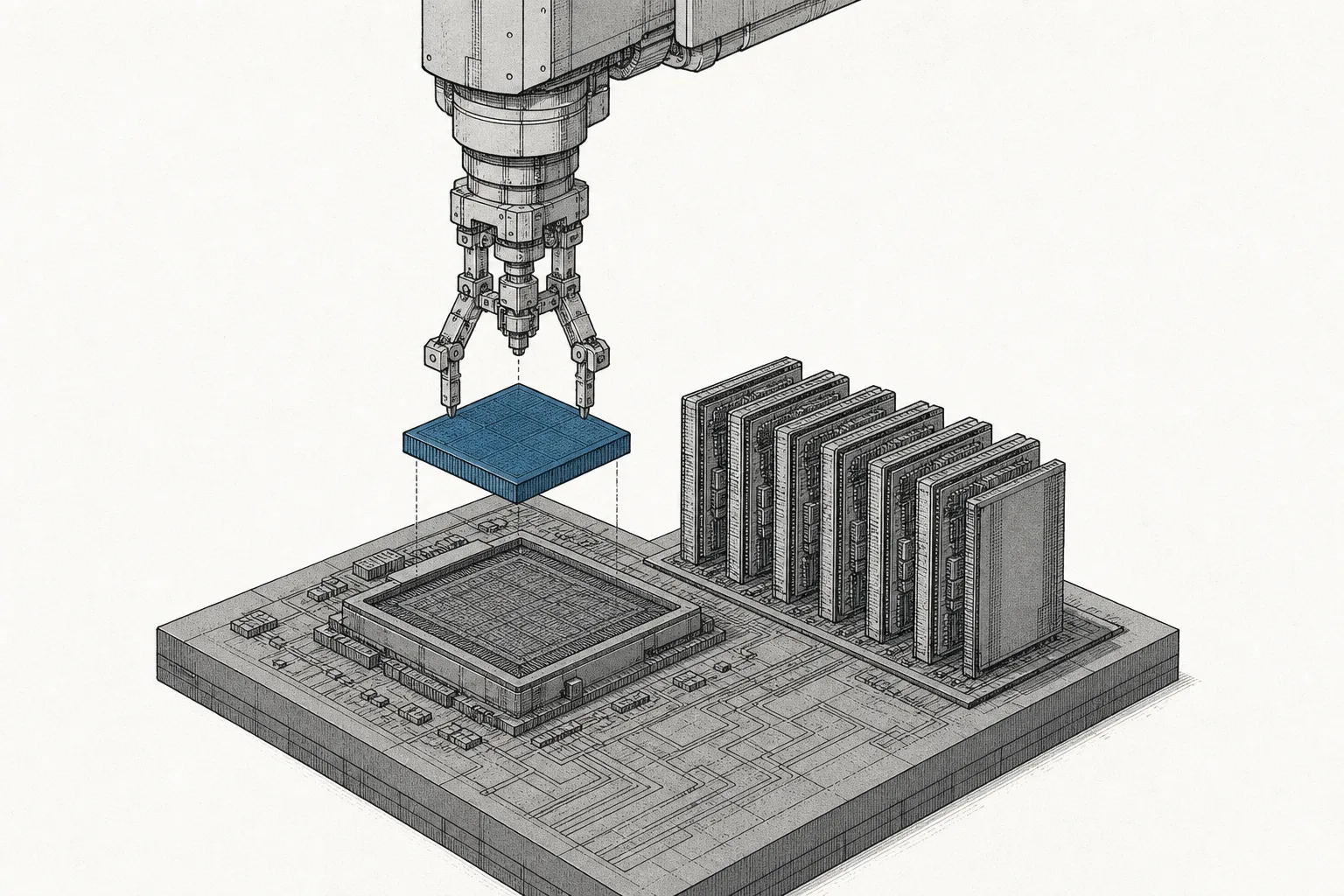
Why split it into two jobs? Because a modern AI chip is no longer a single block of silicon. It's a "chip assembled from many pieces" — a GPU (the computing brain) in the middle, surrounded by several stacks of HBM memory that have to sit extremely close to feed it data fast enough. All of it sits on a thin silicon sheet that acts as a "wiring bridge" connecting every piece. Putting these pieces together so they work as one is "advanced packaging," and TSMC's most famous technique is called CoWoS — whether the computing block in the middle is a GPU or a tech giant's custom chip (an ASIC), it all has to go through this same assembly.
On the megatrend map, this node is a leaf under AI Compute & Accelerator Silicon within the big trend Artificial Intelligence. If its siblings like GPU and HBM are the "pieces," this node is the one that makes those pieces and assembles them together — the last gate before an AI chip leaves the factory.
Foundry = a contract chip-manufacturing factory that builds transistors onto a wafer to the customer's design (TSMC is number one) · Advanced packaging = assembling several chips into one package, instead of placing them one at a time, so the pieces sit closer and communicate faster · CoWoS (Chip-on-Wafer-on-Substrate) = TSMC's advanced-packaging technique that places the GPU and HBM onto a middle silicon sheet (interposer) and assembles them into one AI chip.
02Why it matters — CoWoS is the real bottleneck of the AI boom
Here's a common misconception: people think if you want more AI chips, you just have NVIDIA design more. But the truth is — NVIDIA can design without limit; what it can't keep up with is "making" and "assembling" them. And the most stuck point isn't transistor manufacturing (TSMC keeps up fairly well) but the final assembly — CoWoS.
Here's why. One AI chip needs the GPU placed alongside several stacks of HBM on an interposer that's several times bigger than normal. The work is delicate and slow, and you can only make so many per month. That makes TSMC the "real faucet" — at the end of 2024, TSMC's CoWoS capacity was about 35,000 wafers a month, accelerating to ~75,000/month by the end of 2025, with a target of ~125,000–130,000/month by the end of 2026 — nearly 4x in under two years. And it's still not enough. TSMC's own executives say CoWoS capacity is "very tight and fully booked out through 2026." All advanced packaging is booked out through 2027, with lead times of 52–78 weeks.
Just as important, the most advanced manufacturing is concentrated in one company. In 2026, TSMC controls more than 90% of the advanced-node manufacturing market that AI chips need — meaning nearly every top AI chip in the world, whether NVIDIA's, AMD's, Google's, or Amazon's, is made at TSMC alone. And because AI is sucking in so much advanced capacity, revenue from high-performance computing (HPC, which includes AI chips) has jumped to 58% of TSMC's total revenue in 2025, and will pass 60% in 2026.
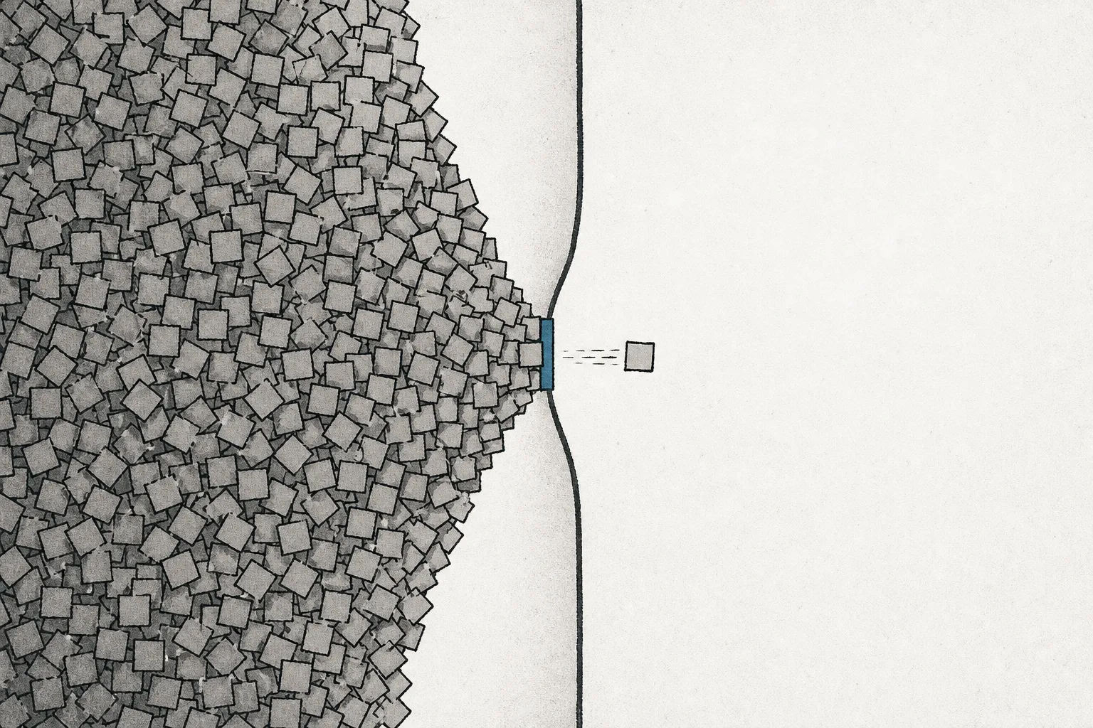
This is why this node matters quietly but powerfully: anyone who wants to understand why AI chips are "in short supply" even though demand overflows has to look at this layer — because the bottleneck is in the capacity to build and assemble, not in the ideas or the design.
03How it works — from GPU + HBM to a single package
The heart of advanced packaging is a simple question: how do you get the GPU and the HBM memory as close together as possible? Because the closer they are, the faster data flows and the less power it burns. If you put the HBM far away on a circuit board (PCB) like a normal computer, bandwidth drops sharply and the GPU can't run at full strength. TSMC's answer is CoWoS — let's walk through, step by step, how one AI chip gets assembled.
The interposer in the middle is the invisible star. It's a thin silicon sheet with high-density wiring and "through-silicon via" (TSV) holes drilled through it, letting the GPU talk to the HBM at speeds of several terabits per second — many times faster than going through a normal circuit board. The catch is that the interposer for an AI chip keeps getting bigger (several times past the standard wafer size); the bigger it is, the harder to make and the easier to ruin — that's the technical reason CoWoS is a bottleneck.
CoWoS is a "2.5D" form of assembly — placing the pieces side by side on the interposer (not stacked). The next stage is 3D — stacking chips directly on top of each other and joining them with atom-level "hybrid bonding." TSMC's 3D technique is called SoIC (System on Integrated Chips), which gets the pieces even closer, raising both speed and density — the direction the newest AI chips are heading.
04Where it sits in the ecosystem
If you look at the whole AI-chip layer as one production line, this node is the endpoint where every piece converges — the gate where the design becomes a real thing. It's inseparably connected to its neighbors.
- Assembling GPU with HBM: these two are the main materials CoWoS assembles. If either one runs short — GPU short or HBM short — the assembly line stops. So the CoWoS bottleneck, the HBM bottleneck, and the GPU bottleneck are one tangled problem
- The AI angle of Foundry and Advanced Packaging: chip-industry manufacturing and assembly serve many kinds of customers, but AI is the fastest-growing and highest-paying one right now, to the point that HPC has become 58% of TSMC's revenue — this node is the "AI branch" of those two stories in the Semiconductors trend
- Draws power from Energy Transition & Power: foundry and packaging plants consume enormous amounts of electricity and water, so expanding capacity ties directly to how ready each region's power grid is
- Depends on Critical Materials & Supply Chain: advanced packaging needs high-quality substrates, special chemicals, and rare materials — so this node is sensitive to strains in the world's raw-material supply chain
05Where it stands now
The current picture can be summed up in one sentence: TSMC holds an almost complete grip on both manufacturing and assembly of the most advanced AI chips. At the end of 2025, TSMC began volume production of 2-nanometer (2nm) chips at good yields and kept accelerating CoWoS assembly capacity, with its biggest customer being NVIDIA, which has already booked over 70% of 2025's CoWoS-L assembly capacity to feed its Blackwell chips. The rest is split among AMD, Broadcom, Marvell, and others.
Rivals are trying to catch up, but still trail by a fair distance. Intel, with its own foundry, has pushed 18A-chip yields above 60% and started winning some outside customers. Meanwhile Samsung, long the number two in advanced manufacturing, has stumbled on 2nm-chip yields (believed to be still under 40%) — so the gap between first and second in AI-chip manufacturing is still wide.
On the assembly side, beyond TSMC doing CoWoS itself, there's a group of contract assembly-and-test factories called OSAT, which took roughly 59% of the advanced-packaging market in 2025, led by ASE (number one in the world) and Amkor (number two, about 15% share, roughly $6.3B in revenue in 2024) — both take on the assembly TSMC can't get to or doesn't do itself, and are expanding advanced-assembly capacity to ride the AI wave.
06The road ahead
The first direction is expanding assembly capacity at full tilt. As long as CoWoS is the bottleneck, TSMC and its rivals will keep pouring money into building new assembly plants — the target of ~125,000–130,000/month by the end of 2026 is nearly 4x growth in two years. This is this node's structural tailwind: as long as AI-chip demand overflows, every bit of added assembly capacity just gets booked out.
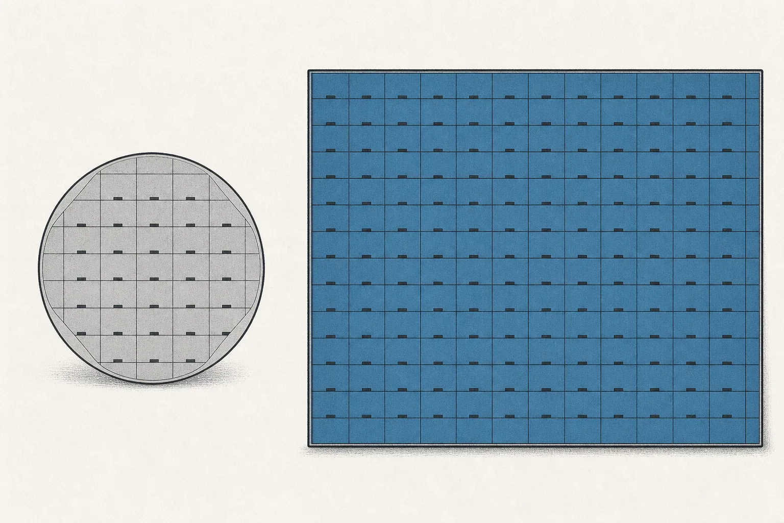
The second direction is moving from round wafers to square panels (panel-level packaging). Today, assembly is done on round wafers, which waste a lot of edge and limit the size. The industry is moving toward assembling on large square panels (like a display) to assemble more pieces per round and handle bigger AI chips — but it requires investing in new production lines costing more than $500 million per line.
The third direction is new materials — glass substrate and 3D bonding. Glass substrate is flatter and more heat-resistant than the old materials, helping assemble big chips more precisely. Meanwhile 3D chip stacking (SoIC, hybrid bonding) brings the GPU and memory even closer — both are the "next generation" of assembly that will define AI chips over the next few years.
07Challenges & risks
The first risk is concentration in Taiwan. With over 90% of the most advanced AI chips made and assembled by TSMC, whose main production base is in Taiwan, geopolitical risk and natural disasters aren't distant concerns. If this single point stumbles, the world's whole AI-chip supply chain shakes instantly. TSMC is trying to spread the risk by building plants in the US (investing up to $165 billion total in Arizona), but moving advanced-assembly capacity along with it takes years.
The second risk is an assembly bottleneck that can't keep up with demand. Even as TSMC expands CoWoS nearly 4x, many analysts still think it may be not enough for demand growing even faster. The result is AI chips staying in short supply, prices high, and smaller customers unable to get in line ahead of the big ones — this bottleneck becomes the thing that decides who gets AI chips first.
The third risk is dependence on a few customers and partners. With NVIDIA booking over 70% of assembly capacity, this layer's revenue is tied to the AI spending of a few deep-pocketed customers. If AI investment slows, or demand that looked bottomless starts to fill up, the assembly capacity just built at enormous cost could be left in surplus overnight — a high-margin business, but one chained to a volatile investment cycle.
In short: this node is the answer to a question many people overlook — "who really makes AI chips?" The answer isn't NVIDIA, it's TSMC and the few assembly factories that put GPU and HBM together into one piece. As long as CoWoS assembly is the slowest, scarcest point, this layer remains one of the most powerful bottlenecks in the entire AI economy.