Megatrend · Artificial Intelligence
Before any AI chip exists, it has to pass through the "software" and "off-the-shelf blocks" of just a few companies
Everyone knows NVIDIA. But few people know that before any GPU or custom chip can be made, it first has to be "designed" with specialized software called EDA — and is usually assembled from "off-the-shelf blocks" called IP, like Arm's processor cores. This node is the deepest layer of all, the "shovels and picks of the people selling shovels" — and they're selling like never before, because every company is now rushing to design its own AI chip. The game-changer: it's started using AI to design the chips itself.
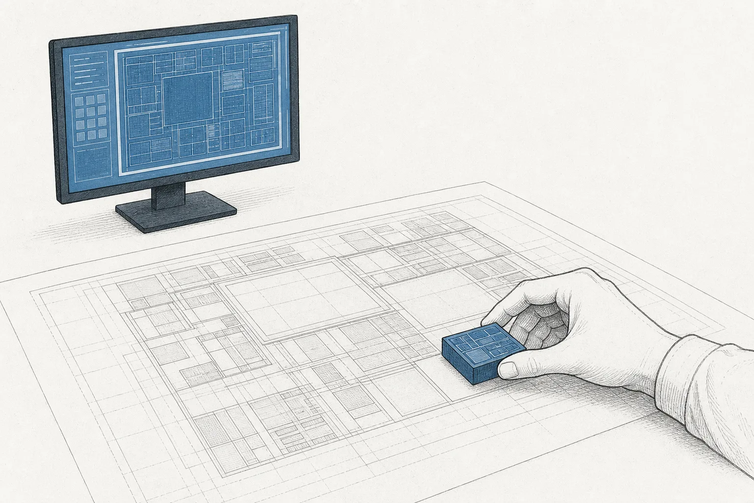
01What it is (design tools + IP blocks)
Picture building a skyscraper. Before anyone lays a single brick, two things always come first — (1) design software (CAD) that the architect uses to draw and simulate every floor, and (2) off-the-shelf parts like elevators or steel frames, bought ready-designed from specialists so you don't reinvent them every time. The chip world works exactly the same way, and this node is those two things.
The first is EDA (Electronic Design Automation) — the software engineers use to design, simulate, and verify chips with tens of billions of transistors. Without EDA, no human could design a modern chip by hand — it'd be like drawing a map of an entire country by counting each tree one at a time. The second is Semiconductor IP (pre-designed intellectual-property blocks) — instead of every company inventing a "processor core" from scratch, they buy a ready-made license and assemble it in, like Arm's CPU core or the data-connection blocks (interface IP) used to plug in HBM and PCIe.
On the megatrend map, this node is the deepest leaf under AI Compute & Accelerator Silicon, within the big trend Artificial Intelligence. While siblings like GPU & Merchant Accelerators and Custom Silicon / ASIC are the "actual chips," this node is the layer that comes before all of them — the tools and intellectual raw material used to build those chips. That's why you can call it the "shovels and picks of the people selling shovels."
EDA = automated software for designing, simulating, and verifying a chip's circuits (for example, synthesis turns code into circuits, place-and-route arranges the transistors, and verification hunts for bugs before manufacturing) · IP (Semiconductor IP) = a pre-designed, pre-tested circuit block sold as a "license" to assemble into a chip, like Arm's CPU core · Tape-out = the point where a chip design is complete and sent to the factory (foundry) to be made — like "sending the manuscript to the printer"
02Why it matters — every AI chip passes through this gate first
The first reason is that it's the bottleneck furthest "upstream." Whether the AI chip war ends with NVIDIA's GPUs, AMD's MI chips, or Google and Amazon's custom chips — all of them are designed on EDA software, and most are assembled from the same IP blocks. So this node "collects a toll" from every camp in the arena, without having to guess who wins.
The second reason is that the custom-chip boom is driving this layer's demand directly. There used to be only a few chip-design companies, but today every cloud giant — Google, Amazon, Microsoft, Meta, OpenAI — is pouring effort into designing its own AI chip (see Custom Silicon / ASIC). The more people design chips, the more the sellers of design tools and IP blocks sell. That's why Arm reported its licensing revenue jumped about 70% in the first quarter of fiscal 2025, riding the custom-chip demand.
The third reason is that the value concentrates in "knowledge that's hard to copy." The global EDA market isn't large compared to the chip market (around $12–15 billion a year), yet it props up the entire $600-billion-plus semiconductor industry — software worth tens of billions becomes the key that opens the door to a multi-trillion-dollar core industry. This is a business that's truly "small but mighty."

03How it works (from spec to tape-out)
Designing one AI chip doesn't happen in a single step — it's a conveyor belt that flows from "idea" to "the manuscript sent to the factory." This node sells tools and parts at nearly every point on that belt. Let's walk through it step by step.
What makes this layer "hard" is that modern AI chips are so complex that humans can't keep up — tens of billions of transistors, with every bug needing to be found before tape-out, because a missed mistake on something already manufactured costs tens of millions of dollars to fix. The decades of accumulated know-how in "laying out transistors to be the fastest and most power-efficient" is the wall that keeps the number of companies that can do full-stack EDA down to just a few.
It's the same on the IP side. Designing a CPU core that's stable and compatible with all the world's software takes decades, so buying an Arm core license and slotting it in is vastly faster and safer than rolling your own. And Arm gets paid twice: a license fee at the start of the design, and a royalty collected on every chip sold. The more chips its customers sell, the bigger Arm's cut.
04Where it sits in the ecosystem
If you picture the whole life of an AI chip as a river, this node is the furthest upstream — it comes before everything and feeds everyone downstream.
- Feeds GPU and Custom Silicon / ASIC directly: both NVIDIA's GPUs and the cloud giants' custom chips are designed on EDA and assembled from IP blocks — especially ASICs, whose design teams are often smaller and so lean especially hard on ready-made IP and automation tools. Every new custom chip is a new order for this layer
- It's the "design department" of the whole Semiconductors — Logic, Foundry & IP industry: EDA and IP aren't used only for AI chips but for every kind of chip — phones, cars, IoT. This lesson views it through the "AI lens," but if you want the whole-industry picture of EDA/IP, see Semiconductors
- Hands off to Foundry & Advanced Packaging: the destination of tape-out is the factory. EDA tools have to mesh tightly with TSMC/Samsung's manufacturing processes — design and manufacturing are an inseparable pair
- Connects with HBM & AI Memory: plugging HBM memory into a chip needs specialized "interface IP" (like Rambus's) — the point where an IP block decides how fast a chip can be fed data
05Where it stands now
The most shocking thing about the EDA layer is the "three companies control nearly the whole world" level of concentration — Synopsys at about 31%, Cadence about 30%, and Siemens EDA about 13%, together controlling over 70% of the market. Synopsys and Cadence in particular are a "duopoly" almost no one can break into for full-stack design tools — customers can barely switch, because their teams and libraries have been tied to the same tools for years.
2025 saw the biggest deal in the history of design software: in July, Synopsys closed its $35 billion acquisition of Ansys, folding physics simulation into EDA — expanding its addressable market (TAM) to about $31 billion and bringing Synopsys's total revenue (including Ansys) to around $8 billion in 2025. Cadence is at about $5.3 billion.
On the IP side, the star is Arm. In fiscal 2025 its total revenue reached ~$4 billion, and a key milestone was that royalty revenue ($2,168 million) overtook licensing revenue for the first time — a sign that chips using Arm cores are now being made and sold in enormous volumes. Its CSS (Compute Subsystems) program, which helps customers finish a chip design in half the time, has already won 21 licenses from 12 major tech companies by early 2026 — nearly every cloud giant making custom chips relies on Arm's cores.
There are also important specialist players, such as Keysight (test and simulation tools), Rambus (interface IP for high-speed memory), and CEVA (IP for AI/signal work) — each holding its own deep, hard-to-copy niche.
06The road ahead — when AI designs the chips itself
The first direction is the industry's most beautifully "circular" story: AI designing AI chips right back. Modern EDA tools embed AI to help find the best way to lay out transistors — faster, more power-efficient, with fewer engineers. Synopsys's DSO.ai has already passed 100 production tape-outs, while Cadence launched Cerebrus AI Studio, which claims to speed up designing a whole SoC by about 5× — chip-design tools have become both "the seller to the AI era" and "a user of AI" at the same time.
The second direction is that the royalty model compounds. The more Arm and other IP sellers have their cores in chips, every chip made and sold pays a royalty back — revenue that grows with the volume of chips worldwide, not just the number of new deals. In an era where every device embeds AI, the base of royalty-paying chips keeps expanding.
The third direction is the arrival of chiplets and open standards. Modern chips are starting to be assembled from several "small chips" (chiplets) joined together, instead of cast as one block — making interface IP (the blocks that connect chiplets, like the UCIe standard) much more valuable. There's also the open-architecture wave of RISC-V as an alternative to Arm cores — opening room for newcomers like Andes and VeriSilicon to break into the IP market.
07Challenges & risks
The first risk is exports to China becoming a political hostage. Because EDA is the upstream bottleneck for all chips, it's also a weapon in the tech war. In May 2025, the U.S. ordered Synopsys, Cadence, and Siemens EDA to obtain a license before every sale to China — Synopsys gets about 16% of revenue from China (~$1 billion) and Cadence about 12% (~$550 million), so they were shaken instantly. Even though the order was reversed in July 2025 after China retaliated by restricting rare earths, the episode showed that a big chunk of this layer's revenue hangs on politics that can flip in a few weeks.
The second risk is concentration and reliance on a few customers. With the EDA market held by three companies and Arm the big player on the IP side, this level of concentration means that if major customers (a handful of cloud giants) slow their chip-design plans, or lean more on open alternatives like RISC-V, the leaders' revenue is shaken too — and Arm's own success rides on a few big customers who are now both partners and rivals.
The third risk is the double-edged sword of AI designing chips. AI tools that speed up design are a good selling point, but if they make "chip design so much easier" that small teams or startups can do it themselves, the wall that protected the big three could get lower. In the short term it's a tailwind, but in the long term the technology they built could open the door to new rivals — the classic dilemma of a leader who has to rush to grab the market it's revolutionizing.
In short: this node is the deepest and quietest layer of the AI era — no one sees it, but every chip passes through. It sells design tools and ready-made blocks to every camp, collects a toll from the whole arena, and is now using AI to design AI chips in a loop that accelerates the entire industry. Understand this layer, and you understand who's quietly taking a cut behind the scenes "before" every AI chip is even born.